in HWinfo i can see the two first core go at 3.5 Ghz all other are in 3.1Ghz but in Cbr20 they fall bellow 3Ghz but power is in the 230W while I think on my other board thy were in the 3.1 3.2 Ghz range. With 3.9 bios every time I get a better multithread score my single score drop and never really get close to the Asrack board will drop back to bios 3.1 and see. (there could probably be a firmware fix for specter or meldown or soemthing else at play also maiby cpu governer limiting turbo or maiby AVX loads?)
VRM modify ICC_MAX to run high TDC/TDP OEM processors
- Thread starter RolloZ170
- Start date
Notice: Page may contain affiliate links for which we may earn a small commission through services like Amazon Affiliates or Skimlinks.
i have tested 8222CL & 8175M on BIOS 3.8a with no such issues, after that i sold my X11SPM-F.in HWinfo i can see the two first core go at 3.5 Ghz all other are in 3.1Ghz but in Cbr20 they fall bellow 3Ghz but power is in the 230W while I think on my other board thy were in the 3.1 3.2 Ghz range. With 3.9 bios every time I get a better multithread score my single score drop and never really get close to the Asrack board will drop back to bios 3.1 and see. (there could probably be a firmware fix for specter or meldown or soemthing else at play also maiby cpu governer limiting turbo or maiby AVX loads?)
sure newer microcodes can cause this. ASRock's BIOS 2.10 includes very very old with microcode from 2019.

try BIOShad tryed the IPMI and had the same error. WIll try 3.6 thak you


can you compare the all core clock of the two boards ? use CPU-Z stress cpu to load (std.setting)Getting closer using bios 3.4 can get nicer single core speed and still somewhat good multithread scores. Not as hight as the Asrock board but getting closer.
i think the ASRock allows more time to exceed TDP (PL1 time window)
and
i can make acustom BIOS 3.4 later today, if you have the time and wiling to check this.
You are going above and beyond. I was also thinking it is probably a PL1 PL2 thing. Unfortunally i do not have the asrack board with me a this time only took the supermicro one to thinking with over the weekend.can you compare the all core clock of the two boards ? use CPU-Z stress cpu to load (std.setting)
i think the ASRock allows more time to exceed TDP (PL1 time window)
and
i can make acustom BIOS 3.4 later today, if you have the time and wiling to check this.
But if you are really intereested I will make time to get you those numbers a a later time the least I can do with all the help you provided to me and others.
they are castrated to 3+1 VRM, not way for anything over 165W. some seller have pictures of the 5+1 variant but ship the 3+1.Anyone managed to find the required I2C pin headers on the "crippled" 85W locked Quanta T42S-2U node boards?
It has TPS53679.
and if they have BIOS TDP lock, you have to do a BIOS modd too, works with clamp and USB programmer because BIOS is signed.
Yep, I'd be very happy with 125W TDP support.they are castrated to 3+1 VRM, not way for anything over 165W. some seller have pictures of the 5+1 variant but ship the 3+1.
and if they have BIOS TDP lock, you have to do a BIOS modd too, works with clamp and USB programmer because BIOS is signed.
I could not find the datasheet of the VRM FETs (3 x 59953MC and 1 x 59954MC), but I guess they are 35-40A max, so ~160A total, which is 144W at 0.9V. That would be enough for me to run 6138 and such CPUs.
AFAIK the TDP lock is NOT in the BIOS, because some owners already tried various BIOS versions that support any CPU in the "normal" T42S board, but still does not post with the crippled board.
So I think BIOS mod is not necessary, only VRM controller mod. Or am I missing something?
maybe the VRM units ICC_MAX is 190Amps. like on the supermicro X11DPLAFAIK the TDP lock is NOT in the BIOS, because some owners already tried various BIOS versions that support any CPU in the "normal" T42S board, but still does not post with the crippled board.
So I think BIOS mod is not necessary, only VRM controller mod. Or am I missing something?
228A is std. equals to CPU TDC value.
3+1I could not find the datasheet of the VRM FETs (3 x 59953MC and 1 x 59954MC), but I guess they are 35-40A max, so ~160A total, which is 144W at 0.9V. That would be enough for me to run 6138 and such CPUs.
3 are VCCCore, 1 is VCCIA IntelAgent.
all scalables use FIFR, the VRM delivers 1.6-1.7Volt constant. a FET with max. 40A can not deliver constant 40A (PWM)
changing the ICC_MAX does not change phase current or something similar. change ICC_MAX just allows to start.
edit:
CSD59953Q5MC datasheet only under NDA.
Last edited:
yeah only 3 phases for Vcore then. I am not familiar with FIVR. Then it's around 90A for Vcore, which gives around 150W @1.7V.3+1
3 are VCCCore, 1 is VCCIA IntelAgent.
all scalables use FIFR, the VRM delivers 1.6-1.7Volt constant. a FET with max. 40A can not deliver constant 40A (PWM)
changing the ICC_MAX does not change phase current or something similar. change ICC_MAX just allows to start.
edit:
CSD59953Q5MC datasheet only under NDA.
Yes I also found these mosfets are customer specifics super top secret sh*t.
Datasheet is not really important as I can monitor the mosfets overload with my infra cam. If they get hot, I know there is trouble
")
Also have to put a heatsink on them as they are also missing.
So next step is to find the pins for I2C. Worst case I'll have to solder directly on the IC legs, but I am sure they can be found somewhere.
Is there pinout diagram for the TPS53679? Found it
Last edited:
OK, for all who want to run high TDC OEM processors on motherboards don't support this by default.
currentyl supported are the following motherboards:
Supermicro X11SPM-(T/P)F
Supermicro X11SPi-NT
Supermicro X11SPL-F
Supermicro X11DPi-N(T)
Supermicro X11DPH-i/T
Supermicro X11DPG-QT
intel S2600BP?
intel S2600WF?
intel S2600ST?
Dell Precision T7820
Dell Precision T7920
Dell Precision R7920
Dell PowerEdge T640
Dell PowerEdge R640
Dell PowerEdge R740
HPE Proliant DL380 Gen10
HPE Proliant DL360 Gen10
The Thermal Design Current(TDC) of those processors is 255A, std.default is 228A(TDP=165-205W) and lower.
You can see this TDC value with AIDA, HWinfo does not show this parameter or as PL4.
View attachment 26505
actualy there are three ways to do this, except for boards with PXE1610C ( only supported by MCP2221a )
1) MCP2221a (Adafruit)
i made a c# console app for automatic programming ( MCP2221a_iccmax_FF(18122023).7z ) vrm TPS53679/PXE1610C/MP2955A
(if you have concerns using my exe on your system: use iLSpy to see/get the c# sourcecode of them, and recomplie your own)
typical usage(cmd window)
"MCP2221a_iccmax_FF -MP2955A 20"
or
"MCP2221a_iccmax_FF -PXE1610C 60"
or
"MCP2221a_iccmax_FF -TPS53679 58"
2)
only MP2955A used in
X11SPM-T(P/F)
X11DPi-N(T) rev.2.x and up
and others
you need I2C interface MPS EVKT-USBI2C-02:
MPS Software V4.5.11 ( if you don't get the Software with MP2955A support, PM me )
3) only for mboards use MPS MP2955A and TI TPS53679
Note:We need the ElmorLabs EVC2SX/EVC2SE and the Software EVC2 1.0.1.13
I have made a device-xml for the EVC2 Software, MP2955A_PMBUS.xml
put it in the folder /I2C_DEVICES and delete all other files.
I have made a device-xml for the EVC2 Software, TPS53679_PMBUS.xmlCode:<?xml version="1.0" encoding="utf-8"?> <EVC2> <!-- Application metadata --> <Application> <SoftwareVersion>12</SoftwareVersion> <FileVersion>6</FileVersion> </Application> <!-- Device specification --> <Device> <Name>MP2955A (PMBus)</Name> <Class>1</Class> <BusType>1</BusType> <BusSpeed>100</BusSpeed> <Address Type="Range"> <Start>10</Start> <End>40</End> </Address> <Detect Type="RegisterMatch"> <Register> <Command>BF</Command> <Length>2</Length> <Data>2555</Data> <!-- MPS MP2955A, 2556=MP2956A,2558=MP2958A --> </Register> </Detect> <Constant> <!-- Read once --> </Constant> <Status> </Status> <Configuration><!-- Read/Write options --> <Item> <Name>ICC_MAX</Name> <PreExec> <Command>00</Command><!-- select Page 0 --> <Data>00</Data> </PreExec> <Register Type="List" Restrict="WriteOnly"> <Command>EF</Command> <Length>1</Length> <Data Desc="min.190A">BE</Data> <Data Desc="def.228A">E4</Data> <Data Desc="max.255A">FF</Data> </Register> </Item> <Item> <Name>STORE_USER_ALL</Name> <Register Type="List" Restrict="WriteOnly"> <Command>15</Command> <Length>0</Length> <Data Desc="No">0</Data> <Data Desc="Yes">1</Data> </Register> </Item> </Configuration> <Monitoring> <Item> <Name>MFR_ICC_MAX</Name> <Register Type="Math"> <Command>EF</Command> <Length>1</Length> <Math> <Factor>1</Factor> <Unit>A</Unit> <Format>F1</Format> </Math> </Register> </Item> <Item> <Name>Output Current</Name> <Register Type="Math"> <Command>8C</Command> <Length>2</Length> <StartBit>0</StartBit> <EndBit>10</EndBit> <Math> <Factor>0.25</Factor> <Unit>A</Unit> <Format>F1</Format> </Math> </Register> </Item> </Monitoring> </Device> </EVC2>
Code:<?xml version="1.0" encoding="utf-8"?> <EVC2> <!-- PMBus Device TPS --> <!-- Application metadata --> <Application> <SoftwareVersion>12</SoftwareVersion> <FileVersion>6</FileVersion> </Application> <!-- Device specification --> <Device> <Name>TPS53679 (PMBus)</Name> <Class>1</Class> <BusType>1</BusType> <BusSpeed>100</BusSpeed> <Address Type="Range"> <Start>10</Start> <End>70</End> </Address> <Detect Type="RegisterMatch"> <Register Type="Hex" AccessMethod="Normal"> <Command>AD</Command> <!-- IC_DEVICE_ID = 0xAD --> <Length>2</Length> <Data>7901</Data> <!-- 7901 = tps53679 --> </Register> </Detect> <Constant> <!-- Read once --> <Item> <Name>IOUT_MAX</Name> <PreExec> <Command>00</Command><!-- select Page 0 --> <Data>00</Data> </PreExec> <Register Type="Math" AccessMethod="Normal"> <Command>DA</Command> <Length>2</Length> <StartBit>0</StartBit> <EndBit>7</EndBit> <Math> <Factor>1</Factor> <Unit>A</Unit> <Format>F0</Format> </Math> </Register> </Item> <Item> <Name>IOUT_OC_FAULT_LIM</Name> <PreExec> <Command>00</Command><!-- select Page 0 --> <Data>00</Data> </PreExec> <Register Type="Math" AccessMethod="Normal"> <Command>46</Command> <Length>2</Length> <StartBit>0</StartBit> <EndBit>10</EndBit> <Math> <Factor>1</Factor> <Unit>A</Unit> <Format>F0</Format> </Math> </Register> </Item> <Item> <Name>IOUT_OC_WARN_LIM</Name> <PreExec> <Command>00</Command><!-- select Page 0 --> <Data>00</Data> </PreExec> <Register Type="Math" AccessMethod="Normal"> <Command>4A</Command> <Length>2</Length> <StartBit>0</StartBit> <EndBit>10</EndBit> <Math> <Factor>1</Factor> <Unit>A</Unit> <Format>F0</Format> </Math> </Register> </Item> </Constant> <Status> </Status> <Configuration> <!-- Read/Write options --> <Item> <Name>IOUT_MAX</Name> <PreExec> <Command>00</Command> <!-- select Page 0 --> <Data>00</Data> </PreExec> <Register Type="List"> <Command>DA</Command> <Length>2</Length> <StartBit>0</StartBit> <EndBit>7</EndBit> <Data Desc="low.190A">BE</Data> <!-- X11DPL-i standard --> <Data Desc="def.228A">E4</Data> <!-- standard except X11DPL-i --> <Data Desc="max.255A">FF</Data> </Register> </Item> <Item> <Name>STORE_DEFAULT_ALL</Name> <Register Type="List" Restrict="WriteOnly"> <Command>11</Command> <Length>0</Length> <Data Desc="No">0</Data> <Data Desc="Yes">1</Data> </Register> </Item> </Configuration> <Monitoring> <Item> <Name>IOUT_MAX</Name> <PreExec> <Command>00</Command> <!-- select Page 0 --> <Data>00</Data> </PreExec> <Register Type="Math"> <Command>DA</Command> <Length>2</Length> <StartBit>0</StartBit> <EndBit>7</EndBit> <Math> <Factor>1</Factor> <Unit>A</Unit> <Format>F1</Format> </Math> </Register> </Item> <Item> <Name>Output Current</Name> <Register Type="Math"> <Command>8C</Command> <Length>2</Length> <StartBit>0</StartBit> <EndBit>10</EndBit> <Math> <Factor>0.25</Factor> <Unit>A</Unit> <Format>F1</Format> </Math> </Register> </Item> </Monitoring> </Device> </EVC2>
If you don't have suported CPU(s) to do the modification try it with the high TDC CPU(s), mostly this works,
the system just turns on but you will get no display, the CPU(s) reset is helt low.
you can do now the VRM modification. With supported CPU(s) enter the BIOS and start modifying.
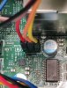
Do not power the X11SPM, install a CPU and connect the EVC2SX or MCP2221a header with a 3 wire Cable to the JVR1 header of the X11SPM
View attachment 26506
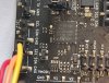
Connect the EVC2SX with the USB Cable to your PC and start the EVC2 Software.
Now you can power on the X11SPM, click on I2C1 and click "Find Devices" the MP2955A should be found and visible under I2C1.
Click on this entry to open the Device:
View attachment 26507
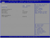
click "Monitoring" to see the value of ICC_MAX.
you can select the standard or max. ICC_MAX in the dropdown menu.
View attachment 26508
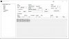
STORE_USER_ALL is to save the setting permanent.
View attachment 26509
With a click at "Apply changes" the new ICC_MAX is written and if you choosed "yes" for STORE_USER-ALL this setting is copied in the NVM of the VRM controller.
View attachment 26510
If you have any questions, ask me.
X11DPi-N(T):
i have successfully modified a X11DPi-N(T) rev. 2.01A to run TDC 255A TDP 240W SKUs(i.e. Amazon AWS customs)
With CPU in both sockets installed the procedure is similar than decribed above, you will see two MP2955A (adr 0x20 and 0x21)
Remove the JVRM1/2 jumpers and connect the I2C :
JVRM1 pin2 = SCL
JVRM2 pin2 = SDA
USB2/3 pin7/8 = GND (or any other GND pin)
X11SPL-F X11SPi-TF X11DPL-i 11DPH-i :
we have successfully modified a X11SPL-F (adr 0x58), X11SPi-TF (adr 0x58), X11SPH (adr 0x58), X11DPL-i (adr 0x58 / 0x60) and X11DPH-i (adr 0x58 / 0x60) to run TDC 255A TDP 240W SKUs(i.e. Amazon AWS customs)
With CPU in both sockets installed the procedure is siliar than decribed above, you will see one or two TPS53679
X11SPL-F & X11SPM-(T)F (may block TDP higher than 165W, Guide to make BIOS 3.8a with 255W support )
X11SPi-TF, X11SPH-nCT(P)F
JVR(M)1 pin1 = SCL
JVR(M)1 pin2 = SDA
JVR(M)1 pin3 = GND
X11DPi:
View attachment 26511View attachment 26512
Remove the JVRM1/2 jumpers and connect the I2C :
JVRM1 pin2 = SCL
JVRM2 pin2 = SDA
USB2/3 pin7/8 = GND (or any other GND pin)
X11DPH:
Remove the JVRM1/2 jumpers and connect the I2C :
JVRM1 pin2 = SCL
JVRM2 pin2 = SDA
T-SGPIO1 Header Pin3/6 = GND (or any other GND pin)
X11DPL-i: (set to 228A to run up to 205W SKU)
Remove the JVRM1/2 jumpers and connect the I2C :
JVRM1 pin2 = SCL
JVRM2 pin2 = SDA
USB2 Header pin7/8 = GND (or any other GND pin)
X11SPL-F and X11SPi-tf do not have JVR or JVRM jumpers. Which jumper should I use to modify them?OK, for all who want to run high TDC OEM processors on motherboards don't support this by default.
currentyl supported are the following motherboards:
Supermicro X11SPM-(T/P)F
Supermicro X11SPi-NT
Supermicro X11SPL-F
Supermicro X11DPi-N(T)
Supermicro X11DPH-i/T
Supermicro X11DPG-QT
intel S2600BP?
intel S2600WF?
intel S2600ST?
Dell Precision T7820
Dell Precision T7920
Dell Precision R7920
Dell PowerEdge T640
Dell PowerEdge R640
Dell PowerEdge R740
HPE Proliant DL380 Gen10
HPE Proliant DL360 Gen10
The Thermal Design Current(TDC) of those processors is 255A, std.default is 228A(TDP=165-205W) and lower.
You can see this TDC value with AIDA, HWinfo does not show this parameter or as PL4.
View attachment 26505
actualy there are three ways to do this, except for boards with PXE1610C ( only supported by MCP2221a )
1) MCP2221a (Adafruit)
i made a c# console app for automatic programming ( MCP2221a_iccmax_FF(18122023).7z ) vrm TPS53679/PXE1610C/MP2955A
(if you have concerns using my exe on your system: use iLSpy to see/get the c# sourcecode of them, and recomplie your own)
typical usage(cmd window)
"MCP2221a_iccmax_FF -MP2955A 20"
or
"MCP2221a_iccmax_FF -PXE1610C 60"
or
"MCP2221a_iccmax_FF -TPS53679 58"
2)
only MP2955A used in
X11SPM-T(P/F)
X11DPi-N(T) rev.2.x and up
and others
you need I2C interface MPS EVKT-USBI2C-02:
MPS Software V4.5.11 ( if you don't get the Software with MP2955A support, PM me )
3) only for mboards use MPS MP2955A and TI TPS53679
Note:We need the ElmorLabs EVC2SX/EVC2SE and the Software EVC2 1.0.1.13
I have made a device-xml for the EVC2 Software, MP2955A_PMBUS.xml
put it in the folder /I2C_DEVICES and delete all other files.
I have made a device-xml for the EVC2 Software, TPS53679_PMBUS.xmlCode:<?xml version="1.0" encoding="utf-8"?> <EVC2> <!-- Application metadata --> <Application> <SoftwareVersion>12</SoftwareVersion> <FileVersion>6</FileVersion> </Application> <!-- Device specification --> <Device> <Name>MP2955A (PMBus)</Name> <Class>1</Class> <BusType>1</BusType> <BusSpeed>100</BusSpeed> <Address Type="Range"> <Start>10</Start> <End>40</End> </Address> <Detect Type="RegisterMatch"> <Register> <Command>BF</Command> <Length>2</Length> <Data>2555</Data> <!-- MPS MP2955A, 2556=MP2956A,2558=MP2958A --> </Register> </Detect> <Constant> <!-- Read once --> </Constant> <Status> </Status> <Configuration><!-- Read/Write options --> <Item> <Name>ICC_MAX</Name> <PreExec> <Command>00</Command><!-- select Page 0 --> <Data>00</Data> </PreExec> <Register Type="List" Restrict="WriteOnly"> <Command>EF</Command> <Length>1</Length> <Data Desc="min.190A">BE</Data> <Data Desc="def.228A">E4</Data> <Data Desc="max.255A">FF</Data> </Register> </Item> <Item> <Name>STORE_USER_ALL</Name> <Register Type="List" Restrict="WriteOnly"> <Command>15</Command> <Length>0</Length> <Data Desc="No">0</Data> <Data Desc="Yes">1</Data> </Register> </Item> </Configuration> <Monitoring> <Item> <Name>MFR_ICC_MAX</Name> <Register Type="Math"> <Command>EF</Command> <Length>1</Length> <Math> <Factor>1</Factor> <Unit>A</Unit> <Format>F1</Format> </Math> </Register> </Item> <Item> <Name>Output Current</Name> <Register Type="Math"> <Command>8C</Command> <Length>2</Length> <StartBit>0</StartBit> <EndBit>10</EndBit> <Math> <Factor>0.25</Factor> <Unit>A</Unit> <Format>F1</Format> </Math> </Register> </Item> </Monitoring> </Device> </EVC2>
Code:<?xml version="1.0" encoding="utf-8"?> <EVC2> <!-- PMBus Device TPS --> <!-- Application metadata --> <Application> <SoftwareVersion>12</SoftwareVersion> <FileVersion>6</FileVersion> </Application> <!-- Device specification --> <Device> <Name>TPS53679 (PMBus)</Name> <Class>1</Class> <BusType>1</BusType> <BusSpeed>100</BusSpeed> <Address Type="Range"> <Start>10</Start> <End>70</End> </Address> <Detect Type="RegisterMatch"> <Register Type="Hex" AccessMethod="Normal"> <Command>AD</Command> <!-- IC_DEVICE_ID = 0xAD --> <Length>2</Length> <Data>7901</Data> <!-- 7901 = tps53679 --> </Register> </Detect> <Constant> <!-- Read once --> <Item> <Name>IOUT_MAX</Name> <PreExec> <Command>00</Command><!-- select Page 0 --> <Data>00</Data> </PreExec> <Register Type="Math" AccessMethod="Normal"> <Command>DA</Command> <Length>2</Length> <StartBit>0</StartBit> <EndBit>7</EndBit> <Math> <Factor>1</Factor> <Unit>A</Unit> <Format>F0</Format> </Math> </Register> </Item> <Item> <Name>IOUT_OC_FAULT_LIM</Name> <PreExec> <Command>00</Command><!-- select Page 0 --> <Data>00</Data> </PreExec> <Register Type="Math" AccessMethod="Normal"> <Command>46</Command> <Length>2</Length> <StartBit>0</StartBit> <EndBit>10</EndBit> <Math> <Factor>1</Factor> <Unit>A</Unit> <Format>F0</Format> </Math> </Register> </Item> <Item> <Name>IOUT_OC_WARN_LIM</Name> <PreExec> <Command>00</Command><!-- select Page 0 --> <Data>00</Data> </PreExec> <Register Type="Math" AccessMethod="Normal"> <Command>4A</Command> <Length>2</Length> <StartBit>0</StartBit> <EndBit>10</EndBit> <Math> <Factor>1</Factor> <Unit>A</Unit> <Format>F0</Format> </Math> </Register> </Item> </Constant> <Status> </Status> <Configuration> <!-- Read/Write options --> <Item> <Name>IOUT_MAX</Name> <PreExec> <Command>00</Command> <!-- select Page 0 --> <Data>00</Data> </PreExec> <Register Type="List"> <Command>DA</Command> <Length>2</Length> <StartBit>0</StartBit> <EndBit>7</EndBit> <Data Desc="low.190A">BE</Data> <!-- X11DPL-i standard --> <Data Desc="def.228A">E4</Data> <!-- standard except X11DPL-i --> <Data Desc="max.255A">FF</Data> </Register> </Item> <Item> <Name>STORE_DEFAULT_ALL</Name> <Register Type="List" Restrict="WriteOnly"> <Command>11</Command> <Length>0</Length> <Data Desc="No">0</Data> <Data Desc="Yes">1</Data> </Register> </Item> </Configuration> <Monitoring> <Item> <Name>IOUT_MAX</Name> <PreExec> <Command>00</Command> <!-- select Page 0 --> <Data>00</Data> </PreExec> <Register Type="Math"> <Command>DA</Command> <Length>2</Length> <StartBit>0</StartBit> <EndBit>7</EndBit> <Math> <Factor>1</Factor> <Unit>A</Unit> <Format>F1</Format> </Math> </Register> </Item> <Item> <Name>Output Current</Name> <Register Type="Math"> <Command>8C</Command> <Length>2</Length> <StartBit>0</StartBit> <EndBit>10</EndBit> <Math> <Factor>0.25</Factor> <Unit>A</Unit> <Format>F1</Format> </Math> </Register> </Item> </Monitoring> </Device> </EVC2>
If you don't have suported CPU(s) to do the modification try it with the high TDC CPU(s), mostly this works,
the system just turns on but you will get no display, the CPU(s) reset is helt low.
you can do now the VRM modification. With supported CPU(s) enter the BIOS and start modifying.
Do not power the X11SPM, install a CPU and connect the EVC2SX or MCP2221a header with a 3 wire Cable to the JVR1 header of the X11SPM
View attachment 26506
Connect the EVC2SX with the USB Cable to your PC and start the EVC2 Software.
Now you can power on the X11SPM, click on I2C1 and click "Find Devices" the MP2955A should be found and visible under I2C1.
Click on this entry to open the Device:
View attachment 26507
click "Monitoring" to see the value of ICC_MAX.
you can select the standard or max. ICC_MAX in the dropdown menu.
View attachment 26508
STORE_USER_ALL is to save the setting permanent.
View attachment 26509
With a click at "Apply changes" the new ICC_MAX is written and if you choosed "yes" for STORE_USER-ALL this setting is copied in the NVM of the VRM controller.
View attachment 26510
If you have any questions, ask me.
X11DPi-N(T):
i have successfully modified a X11DPi-N(T) rev. 2.01A to run TDC 255A TDP 240W SKUs(i.e. Amazon AWS customs)
With CPU in both sockets installed the procedure is similar than decribed above, you will see two MP2955A (adr 0x20 and 0x21)
Remove the JVRM1/2 jumpers and connect the I2C :
JVRM1 pin2 = SCL
JVRM2 pin2 = SDA
USB2/3 pin7/8 = GND (or any other GND pin)
X11SPL-F X11SPi-TF X11DPL-i 11DPH-i :
we have successfully modified a X11SPL-F (adr 0x58), X11SPi-TF (adr 0x58), X11SPH (adr 0x58), X11DPL-i (adr 0x58 / 0x60) and X11DPH-i (adr 0x58 / 0x60) to run TDC 255A TDP 240W SKUs(i.e. Amazon AWS customs)
With CPU in both sockets installed the procedure is siliar than decribed above, you will see one or two TPS53679
X11SPL-F & X11SPM-(T)F (may block TDP higher than 165W, Guide to make BIOS 3.8a with 255W support )
X11SPi-TF, X11SPH-nCT(P)F
JVR(M)1 pin1 = SCL
JVR(M)1 pin2 = SDA
JVR(M)1 pin3 = GND
X11DPi:
View attachment 26511View attachment 26512
Remove the JVRM1/2 jumpers and connect the I2C :
JVRM1 pin2 = SCL
JVRM2 pin2 = SDA
USB2/3 pin7/8 = GND (or any other GND pin)
X11DPH:
Remove the JVRM1/2 jumpers and connect the I2C :
JVRM1 pin2 = SCL
JVRM2 pin2 = SDA
T-SGPIO1 Header Pin3/6 = GND (or any other GND pin)
X11DPL-i: (set to 228A to run up to 205W SKU)
Remove the JVRM1/2 jumpers and connect the I2C :
JVRM1 pin2 = SCL
JVRM2 pin2 = SDA
USB2 Header pin7/8 = GND (or any other GND pin)
you find it in the first page. JVR1 or JVRM1X11SPL-F and X11SPi-tf do not have JVR or JVRM jumpers. Which jumper should I use to modify them?
no jumper.
X11SPL-F & X11SPM-(T)F (may block TDP higher than 165W, Guide to make BIOS with 255W support )
X11SPi-TF, X11SPH-nCT(P)F
JVR(M)1 pin1 = SCL
JVR(M)1 pin2 = SDA
JVR(M)1 pin3 = GND

DEV SCAN OK Found 0 addresses:you find it in the first page. JVR1 or JVRM1
no jumper.
X11SPL-F & X11SPM-(T)F (may block TDP higher than 165W, Guide to make BIOS with 255W support )
X11SPi-TF, X11SPH-nCT(P)F
JVR(M)1 pin1 = SCL
JVR(M)1 pin2 = SDA
JVR(M)1 pin3 = GND
View attachment 34228
Attachments
-
 214.4 KB Views: 10
 -
 203.5 KB Views: 11
 -
 198.4 KB Views: 11
 -
 55.8 KB Views: 11
DEV SCAN OK Found 0 addresses:OK, for all who want to run high TDC OEM processors on motherboards don't support this by default.
currentyl supported are the following motherboards:
Supermicro X11SPM-(T/P)F
Supermicro X11SPi-NT
Supermicro X11SPL-F
Supermicro X11DPi-N(T)
Supermicro X11DPH-i/T
Supermicro X11DPG-QT
intel S2600BP?
intel S2600WF?
intel S2600ST?
Dell Precision T7820
Dell Precision T7920
Dell Precision R7920
Dell PowerEdge T640
Dell PowerEdge R640
Dell PowerEdge R740
HPE Proliant DL380 Gen10
HPE Proliant DL360 Gen10
The Thermal Design Current(TDC) of those processors is 255A, std.default is 228A(TDP=165-205W) and lower.
You can see this TDC value with AIDA, HWinfo does not show this parameter or as PL4.
View attachment 26505
actualy there are three ways to do this, except for boards with PXE1610C ( only supported by MCP2221a )
1) MCP2221a (Adafruit)
i made a c# console app for automatic programming ( MCP2221a_iccmax_FF(18122023).7z ) vrm TPS53679/PXE1610C/MP2955A
(if you have concerns using my exe on your system: use iLSpy to see/get the c# sourcecode of them, and recomplie your own)
typical usage(cmd window)
"MCP2221a_iccmax_FF -MP2955A 20"
or
"MCP2221a_iccmax_FF -PXE1610C 60"
or
"MCP2221a_iccmax_FF -TPS53679 58"
2)
only MP2955A used in
X11SPM-T(P/F)
X11DPi-N(T) rev.2.x and up
and others
you need I2C interface MPS EVKT-USBI2C-02:
MPS Software V4.5.11 ( if you don't get the Software with MP2955A support, PM me )
3) only for mboards use MPS MP2955A and TI TPS53679
Note:We need the ElmorLabs EVC2SX/EVC2SE and the Software EVC2 1.0.1.13
I have made a device-xml for the EVC2 Software, MP2955A_PMBUS.xml
put it in the folder /I2C_DEVICES and delete all other files.
I have made a device-xml for the EVC2 Software, TPS53679_PMBUS.xmlCode:<?xml version="1.0" encoding="utf-8"?> <EVC2> <!-- Application metadata --> <Application> <SoftwareVersion>12</SoftwareVersion> <FileVersion>6</FileVersion> </Application> <!-- Device specification --> <Device> <Name>MP2955A (PMBus)</Name> <Class>1</Class> <BusType>1</BusType> <BusSpeed>100</BusSpeed> <Address Type="Range"> <Start>10</Start> <End>40</End> </Address> <Detect Type="RegisterMatch"> <Register> <Command>BF</Command> <Length>2</Length> <Data>2555</Data> <!-- MPS MP2955A, 2556=MP2956A,2558=MP2958A --> </Register> </Detect> <Constant> <!-- Read once --> </Constant> <Status> </Status> <Configuration><!-- Read/Write options --> <Item> <Name>ICC_MAX</Name> <PreExec> <Command>00</Command><!-- select Page 0 --> <Data>00</Data> </PreExec> <Register Type="List" Restrict="WriteOnly"> <Command>EF</Command> <Length>1</Length> <Data Desc="min.190A">BE</Data> <Data Desc="def.228A">E4</Data> <Data Desc="max.255A">FF</Data> </Register> </Item> <Item> <Name>STORE_USER_ALL</Name> <Register Type="List" Restrict="WriteOnly"> <Command>15</Command> <Length>0</Length> <Data Desc="No">0</Data> <Data Desc="Yes">1</Data> </Register> </Item> </Configuration> <Monitoring> <Item> <Name>MFR_ICC_MAX</Name> <Register Type="Math"> <Command>EF</Command> <Length>1</Length> <Math> <Factor>1</Factor> <Unit>A</Unit> <Format>F1</Format> </Math> </Register> </Item> <Item> <Name>Output Current</Name> <Register Type="Math"> <Command>8C</Command> <Length>2</Length> <StartBit>0</StartBit> <EndBit>10</EndBit> <Math> <Factor>0.25</Factor> <Unit>A</Unit> <Format>F1</Format> </Math> </Register> </Item> </Monitoring> </Device> </EVC2>
Code:<?xml version="1.0" encoding="utf-8"?> <EVC2> <!-- PMBus Device TPS --> <!-- Application metadata --> <Application> <SoftwareVersion>12</SoftwareVersion> <FileVersion>6</FileVersion> </Application> <!-- Device specification --> <Device> <Name>TPS53679 (PMBus)</Name> <Class>1</Class> <BusType>1</BusType> <BusSpeed>100</BusSpeed> <Address Type="Range"> <Start>10</Start> <End>70</End> </Address> <Detect Type="RegisterMatch"> <Register Type="Hex" AccessMethod="Normal"> <Command>AD</Command> <!-- IC_DEVICE_ID = 0xAD --> <Length>2</Length> <Data>7901</Data> <!-- 7901 = tps53679 --> </Register> </Detect> <Constant> <!-- Read once --> <Item> <Name>IOUT_MAX</Name> <PreExec> <Command>00</Command><!-- select Page 0 --> <Data>00</Data> </PreExec> <Register Type="Math" AccessMethod="Normal"> <Command>DA</Command> <Length>2</Length> <StartBit>0</StartBit> <EndBit>7</EndBit> <Math> <Factor>1</Factor> <Unit>A</Unit> <Format>F0</Format> </Math> </Register> </Item> <Item> <Name>IOUT_OC_FAULT_LIM</Name> <PreExec> <Command>00</Command><!-- select Page 0 --> <Data>00</Data> </PreExec> <Register Type="Math" AccessMethod="Normal"> <Command>46</Command> <Length>2</Length> <StartBit>0</StartBit> <EndBit>10</EndBit> <Math> <Factor>1</Factor> <Unit>A</Unit> <Format>F0</Format> </Math> </Register> </Item> <Item> <Name>IOUT_OC_WARN_LIM</Name> <PreExec> <Command>00</Command><!-- select Page 0 --> <Data>00</Data> </PreExec> <Register Type="Math" AccessMethod="Normal"> <Command>4A</Command> <Length>2</Length> <StartBit>0</StartBit> <EndBit>10</EndBit> <Math> <Factor>1</Factor> <Unit>A</Unit> <Format>F0</Format> </Math> </Register> </Item> </Constant> <Status> </Status> <Configuration> <!-- Read/Write options --> <Item> <Name>IOUT_MAX</Name> <PreExec> <Command>00</Command> <!-- select Page 0 --> <Data>00</Data> </PreExec> <Register Type="List"> <Command>DA</Command> <Length>2</Length> <StartBit>0</StartBit> <EndBit>7</EndBit> <Data Desc="low.190A">BE</Data> <!-- X11DPL-i standard --> <Data Desc="def.228A">E4</Data> <!-- standard except X11DPL-i --> <Data Desc="max.255A">FF</Data> </Register> </Item> <Item> <Name>STORE_DEFAULT_ALL</Name> <Register Type="List" Restrict="WriteOnly"> <Command>11</Command> <Length>0</Length> <Data Desc="No">0</Data> <Data Desc="Yes">1</Data> </Register> </Item> </Configuration> <Monitoring> <Item> <Name>IOUT_MAX</Name> <PreExec> <Command>00</Command> <!-- select Page 0 --> <Data>00</Data> </PreExec> <Register Type="Math"> <Command>DA</Command> <Length>2</Length> <StartBit>0</StartBit> <EndBit>7</EndBit> <Math> <Factor>1</Factor> <Unit>A</Unit> <Format>F1</Format> </Math> </Register> </Item> <Item> <Name>Output Current</Name> <Register Type="Math"> <Command>8C</Command> <Length>2</Length> <StartBit>0</StartBit> <EndBit>10</EndBit> <Math> <Factor>0.25</Factor> <Unit>A</Unit> <Format>F1</Format> </Math> </Register> </Item> </Monitoring> </Device> </EVC2>
If you don't have suported CPU(s) to do the modification try it with the high TDC CPU(s), mostly this works,
the system just turns on but you will get no display, the CPU(s) reset is helt low.
you can do now the VRM modification. With supported CPU(s) enter the BIOS and start modifying.
Do not power the X11SPM, install a CPU and connect the EVC2SX or MCP2221a header with a 3 wire Cable to the JVR1 header of the X11SPM
View attachment 26506
Connect the EVC2SX with the USB Cable to your PC and start the EVC2 Software.
Now you can power on the X11SPM, click on I2C1 and click "Find Devices" the MP2955A should be found and visible under I2C1.
Click on this entry to open the Device:
View attachment 26507
click "Monitoring" to see the value of ICC_MAX.
you can select the standard or max. ICC_MAX in the dropdown menu.
View attachment 26508
STORE_USER_ALL is to save the setting permanent.
View attachment 26509
With a click at "Apply changes" the new ICC_MAX is written and if you choosed "yes" for STORE_USER-ALL this setting is copied in the NVM of the VRM controller.
View attachment 26510
If you have any questions, ask me.
X11DPi-N(T):
i have successfully modified a X11DPi-N(T) rev. 2.01A to run TDC 255A TDP 240W SKUs(i.e. Amazon AWS customs)
With CPU in both sockets installed the procedure is similar than decribed above, you will see two MP2955A (adr 0x20 and 0x21)
Remove the JVRM1/2 jumpers and connect the I2C :
JVRM1 pin2 = SCL
JVRM2 pin2 = SDA
USB2/3 pin7/8 = GND (or any other GND pin)
X11SPL-F X11SPi-TF X11DPL-i 11DPH-i :
we have successfully modified a X11SPL-F (adr 0x58), X11SPi-TF (adr 0x58), X11SPH (adr 0x58), X11DPL-i (adr 0x58 / 0x60) and X11DPH-i (adr 0x58 / 0x60) to run TDC 255A TDP 240W SKUs(i.e. Amazon AWS customs)
With CPU in both sockets installed the procedure is siliar than decribed above, you will see one or two TPS53679
X11SPL-F & X11SPM-(T)F (may block TDP higher than 165W, Guide to make BIOS 3.8a with 255W support )
X11SPi-TF, X11SPH-nCT(P)F
JVR(M)1 pin1 = SCL
JVR(M)1 pin2 = SDA
JVR(M)1 pin3 = GND
X11DPi:
View attachment 26511View attachment 26512
Remove the JVRM1/2 jumpers and connect the I2C :
JVRM1 pin2 = SCL
JVRM2 pin2 = SDA
USB2/3 pin7/8 = GND (or any other GND pin)
X11DPH:
Remove the JVRM1/2 jumpers and connect the I2C :
JVRM1 pin2 = SCL
JVRM2 pin2 = SDA
T-SGPIO1 Header Pin3/6 = GND (or any other GND pin)
X11DPL-i: (set to 228A to run up to 205W SKU)
Remove the JVRM1/2 jumpers and connect the I2C :
JVRM1 pin2 = SCL
JVRM2 pin2 = SDA
USB2 Header pin7/8 = GND (or any other GND pin)
Attachments
-
 214.4 KB Views: 4
 -
 203.5 KB Views: 4
 -
 198.4 KB Views: 2
 -
 55.8 KB Views: 3
motherboard was running with compatible CPU while DEV SCAN ?DEV SCAN OK Found 0 addresses:
Intel SR3GF Xeon Gold 5118motherboard was running with compatible CPU while DEV SCAN ?
should work if anything os right. don't know sorry.Intel SR3GF Xeon Gold 5118